Completed
00:00 What is this video about
Class Central Classrooms beta
YouTube videos curated by Class Central.
Classroom Contents
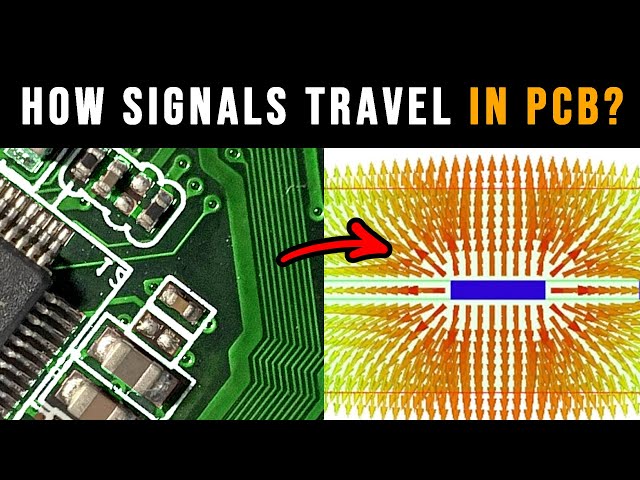
PCB Signal Analysis and Crosstalk Prevention: Understanding Field Behavior and Design Optimization
Automatically move to the next video in the Classroom when playback concludes
- 1 00:00 What is this video about
- 2 00:32 Fields for THICK 2 Layer PCB 1mm / 40mil
- 3 04:47 Fields for THIN 2 Layer PCB 0.1mm / 4mil
- 4 08:44 Fields size compared 1mm vs 0.1mm
- 5 09:11 Crosstalk, fields, currents for 2 Layer PCB two tracks
- 6 16:56 Currents in track
- 7 21:24 Comparing crosstalk in numbers 2 layer PCB
- 8 27:43 Crosstalk for 5W gap between tracks
- 9 35:45 About Simbeor simulation software
- 10 40:57 Fields inside of PCB for one track
- 11 45:00 Fields size compared symmetrical vs. not symmetrical
- 12 45:52 Crosstalk, fields, currents inside of PCB for two tracks
- 13 49:25 Comparing crosstalk in numbers inside PCB
- 14 56:29 Comparing 2 layer vs inside PCB crosstalk for 5W
- 15 1:00:44 Animation of signal travelling through track
- 16 1:04:54 Animation - Moving tracks further from each other
- 17 1:07:14 Signals running through both tracks
- 18 1:10:14 Adding GND track with 2 vias between tracks
- 19 1:12:12 Adding many vias only
- 20 1:13:37 Adding many vias and track
- 21 1:17:12 Importing a real board to Simbeor and analyzing crosstalk
